With the addition of a fourth-generation tabletop Scanning Electron Microscope (SEM), Able’s state-of-the-art suite of analytic tools continues to grow to meet the requirements of high quality finishing for increasingly sophisticated metal parts.
The JCM-7000 NeoScope Benchtop SEM brings a level of precision to surface and elemental analysis that can provide clients with an in-depth understanding of both surface defects and the impact electropolishing can have.
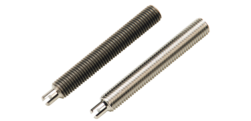
In-house Part Analysis and Reporting for Unmatched Finishing Results
The JCM-7000 NeoScope provides a smart, flexible, and powerful platform for a range of applications from measurement and analysis of surface defects to elemental analysis, as part of Able Electropolishing’s in-house analytic, testing and reporting capabilities.
With part magnification up to 100,000X using a high-resolution W filament source and a combination of secondary and backscatter electron (BSE) detectors alongside high and low vacuum modes, the JCM-7000 can analyze a wide range of sample types and sizes. Automated montage allows for high-resolution imaging over larger areas, and the built-in BSE detector supports live 3D imaging, offering a more intuitive understanding of surface characteristics.
Live Analysis & Rapid Results
The JCM-7000’s energy dispersive X-ray spectroscopy (EDS) enables real-time observation and immediate feedback on material composition, such as iron or chromium content, for quick identification of surface contaminants or embedded particles in the part’s surface.
The JCM-7000 NeoScope can also provide “before and after” imagery, offering clients a detailed picture of surface defects and anomalies at various stages of the process and can serve to validate specifications and results.
Key Features & Industry Impact
- Zeromag simplifies navigation and enhances throughput by providing a seamless transition from optical to SEM imaging
- High-resolution imaging (up to 100,000X magnification) with large depth of field for an incredibly detailed view
- High and low vacuum modes to accommodate a wide variety of sample types
- Large chamber capacity for samples up to 80mm (D) x 50mm (H)
- Advanced functions like Automated Montage and Live 3D Imaging, enhancing the analysis process
- Option to include fully embedded EDS for real-time elemental analysis
Industries such as semiconductor, aerospace and medical device manufacturing rely on high-resolution imaging and detailed material analysis for strict quality control standards. Whether you're inspecting grain structures in metals or identifying microscopic defects, the Able Electropolishing team has the analytic tools and capabilities to ensure high-quality finishing results.
In-House Efficiency & Speed
Having this powerful SEM technology as part of our in-house testing tools allows us to eliminate the need for third-party labs, offering faster, more accurate and more cost-effective material analysis. From design concept through production, Able’s team is committed to delivering metal finishing results that improve the finish, fit and function of your critical metal parts.
As pioneers of the industrial electropolishing process, Able is committed to the continuous improvement of our processes, capabilities and outcomes. Contact a member of our team for free sample electropolishing or schedule a part review to learn more about our custom metal finishing solutions.