 Among the most demanding surface finish requirements of any industry, the specifications, standards and quality assurance processes that cover components used by the semiconductor industry impose metal finishing criteria that leave nothing to chance.
Stainless steel tubing and other components for the manufacture of semiconductors are subjected to detailed surface analysis using Auger Electron Spectroscopy (AES), X-ray Photoelectron Spectroscopy (XPS) and Scanning Electron Microscopy (SEM) to ensure a surface is free of flaws and polished to an Ra level lower than that typically specified for parts used in aerospace and pharmaceutical manufacturing.
- Ultra-High Purity distribution system needed for gas and liquid chemicals used in the manufacture of semiconductors
- 316L Stainless Steel wetted surfaces must be ultrasmooth, ultraclean and able to withstand exposure to highly corrosive gases and liquids
- Need for minimum chromium-to-iron ratio of 1.5:1 and a minimum chromium oxide-to-iron oxide ratio of 2:1.
- Need for ultrasmooth surface, up to 4 Ra, and defect-free finish subject to analysis by Auger Electron Spectroscopy, X-ray Photoelectron Spectroscopy and Scanning Electron Microscopy
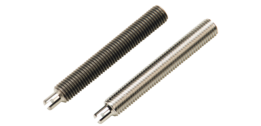
Highly corrosive gasses and liquids used in the manufacture of semiconductors require wetted 316L stainless steel components to be finished with the maximum degree of corrosion resistance.
Electropolishing provides enhanced resistance to corrosion by removing surface defects and enriching the chromium layer of parts manufactured from 316L stainless steel.
By removing a highly precise layer of surface material, electropolishing achieves the chrome-to-iron ratio and chromium-oxide enrichment required for wetted 316L stainless steel used in the manufacture of semiconductor components.
Electropolishing and Chromium Enrichment of 316L Stainless Steel for the Semiconductor Industry
Properly polished electropolished 316L stainless steel has a typical chrome-to-iron ratio of 1.5 or greater, with a maximum depth of chromium enrichment of typically 20 to 25 angstroms.
These results are illustrated in the chart below which shows two 316L stainless steel samples electropolished by Able and analyzed using Auger Electron Spectroscopy (AES).
| Sample Identification | Sample 1 | Sample 2 |
| Oxide Thickness (Å)¹ | 48 Å | 50 Å |
| Adjusted Oxide Thickness (Å)5 | 43 Å | 47 Å |
| Cr Enriched Layer Thickness (Å)7 | 46 Å | 49 Å |
| Cr/Fe Ratio at 10Å6 | 2.2 | 2.1 |
| Max Cr/Fe Depth (Å)² | 3.6 @ 0 Å | 3.1 @ 0 Å |
| Carbon Thickness (Å)4 | 4 Å | 3 Å |
| Surface Fe Oxide Thickness (Å)³ | ND | ND |
| Contaminants | C, N, P, Ca, Na | C, N, P, Ca, Na |
Results of two electropolished samples analyzed by Auger Electron Spectroscopy (AES) and showing the depth of the chrome oxide layer after electropolishing.
Electropolishing enhances the chromium layer to meet requirements that the chromium oxide layer is equal to or greater than 2 nanometers (20 angstroms).
The resulting chromium enrichment leaves parts with significantly improved corrosion resistance.
Semiconductor Component Electropolishing: Pristine Processes for Pristine Parts
- Chromium oxide enrichment at a depth of typically 20-25 angstroms
- Improved chromium to iron ratio for significantly enhanced corrosion resistance
- Microscopically precise removal of outer surfaces containing free iron and embedded contaminants
- Consistent, repeatable results
At Able Electropolishing, semiconductor components arrive at our doors already polished to a high degree, but in need of additional smoothing to adhere to the industry’s exacting standards.
Quality-control for the manufacture of semiconductor parts, many of which will be used only under clean-room conditions, requires extraordinary diligence at every link in the process – not every electropolishing company can achieve this.
A lack of consistency from lot to lot is unacceptable – a fact that has led manufacturers already using electropolishing for their semiconductor components to make the switch to Able.
We are the world’s largest electropolishing specialist and have honed our process over decades of collaboration with engineers and researchers in industries that include aerospace, medical device manufacturing, national laboratories, electronics, automotive and more – in addition to the semiconductor industry.
Alongside our state-of-the-art electropolishing methods, we have further refined our ability to consistently achieve the highest quality results with robotic automation, customized tooling and racking and a prototyping process that includes consultation in the design phase.
Electropolishing: High Quality Results for the Semiconductor Industry
Every step of our process has been meticulously designed to achieve the highest quality results for our clients from start to finish: our rinsing process is another key differentiator for our semiconductor industry clients. Achieving an effective rinse is key to producing ultraclean results. Our process includes multiple cascading rinses with ultrasonics and deionized (DI) water added when necessary. Parts are centrifugally or forced-air dried to ensure that they emerge from our process with an ultrasmooth, ultraclean, and defect and contaminant-free surface. Some items for the semiconductor industry are moved to our class 100 clean bench where they are individually packaged in double bags that have been purged with nitrogen before sealing.
Our work adheres to both semiconductor-specific industry standards (SEMI F19-0185) and general industry standards commonly used like ASTM B912.
See for yourself by taking advantage of our free sample process. We will electropolish your samples at no cost, providing you with a preview of the results you can expect from our high-quality electropolishing process.